AlN Electroabsorption
Problem
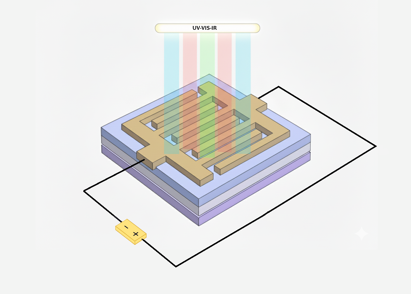
Plasma-enhanced ALD (PEALD) AlN thin films ($\sim$50–100 nm) showed field-dependent UV transmittance changes under applied electric fields up to $\sim200\ \mathrm{MV/m}$.
The modulation reached several percent in transmission, sharply localized near $282\ \mathrm{nm}$.
Question: What physical mechanism produces this field-dependent UV absorption?
Several possibilities existed a priori:
- Crystalline electro-optic effects (Pockels, Kerr)
- Free-carrier absorption
- Field-induced interference from refractive-index changes
- Defect-mediated electroabsorption
My task was not to “find the right mechanism,” but to rule out the ones that were inconsistent with the data.
This was my first experimental spectroscopy analysis project. The measurements existed; the interpretation did not.
What I tried
I started by listing every mechanism I knew that could produce field-dependent optical absorption, then looked for orthogonal measurements that would constrain them.
Step 1: Structural check
X-ray diffraction showed no crystalline peaks above the detection limit.
The AlN films are predominantly amorphous.
Implication:
- Linear electro-optic (Pockels) effect requires non-centrosymmetric crystal symmetry → ruled out.
- Kerr effect scales too weakly at these fields for amorphous AlN → implausible.
Step 2: Spectral range check
I examined visible and near-IR transmittance under bias.
No measurable field-dependent changes were observed outside the UV.
Implication:
- Free-carrier absorption would produce broadband absorption, not a narrow UV-localized response → ruled out.
Step 3: Wavelength specificity
The modulation is sharply peaked near $282\ \mathrm{nm}$ and does not track uniformly across wavelength.
Implication:
- Simple interference from a uniform refractive-index change would affect the spectrum broadly → ruled out.
Step 4: Morphology and field uniformity
AFM showed smooth films with RMS roughness $\sim0.4$–$1\ \mathrm{nm}$, depending on substrate.
Implication:
- Field penetration is approximately uniform across the film thickness.
- The effect is unlikely to be dominated by localized interface roughness or screening.
What survived
After eliminating the alternatives, defect-mediated electroabsorption remained the simplest explanation consistent with all constraints.
Supporting observations (from the manuscript):
- Peak photon energy $\sim4.4\ \mathrm{eV}$ lies well below the AlN band gap ($\sim6.0\ \mathrm{eV}$), consistent with mid-gap defect states.
- PEALD AlN grown at $\sim300^\circ\mathrm{C}$ is known to incorporate defects (e.g., N vacancies, O-related states).
- The absorption coefficient increased from $\sim2.1\times10^3\ \mathrm{cm^{-1}}$ (zero field) to $\sim1.4\times10^4\ \mathrm{cm^{-1}}$ at $200\ \mathrm{MV/m}$.
- The modulation was reversible over repeated bias cycles, ruling out permanent structural changes.
Effective electro-absorption coefficient: \(\alpha_E \approx 6\times10^{-5}\ \mathrm{cm\cdot m/V}\)
This magnitude is consistent with defect-mediated processes in amorphous wide-bandgap semiconductors. :contentReference[oaicite:0]{index=0}
What I could not determine
Specific defect identity
Nitrogen vacancies, oxygen substitution, and aluminum interstitials all introduce states in similar energy ranges. The optical data alone cannot distinguish them.
Defect depth distribution
UV–Vis averages over the optical penetration depth. I could not separate surface, bulk, or interface-localized contributions.
Field-ionization vs. Stark shift
Both mechanisms can produce similar spectral signatures without time-resolved or field-dependent linewidth measurements.
The manuscript explicitly acknowledges these ambiguities rather than assigning a unique defect species. :contentReference[oaicite:1]{index=1}
What I learned
Mechanism identification by elimination is powerful—but only when different measurements constrain different physics.
Here:
- XRD constrained crystal symmetry.
- Spectral range constrained carrier type.
- Wavelength selectivity constrained interference-based explanations.
Without these orthogonal constraints, the result would have been an observation, not an interpretation.
What spectroscopy gives you: constraints, not fingerprints.
What I’d do differently now
If restarting this project:
- Add impedance spectroscopy early to constrain defect depth distributions.
- Vary PEALD conditions intentionally to correlate modulation strength with defect density.
- Use ultrafast pump–probe or field-dependent linewidth measurements to separate Stark shift from field-assisted ionization.
Status: Manuscript submitted (December 2025). First author.
Claim level: Defect-mediated electroabsorption inferred by elimination of alternatives; specific defect species and localization remain unresolved. :contentReference[oaicite:2]{index=2}
Constraint analysis: /constraints/aln-electroabsorption
Methods: UV–Vis, XRD, AFM
Project date: Spring 2025 – Winter 2025
Experience level: First experimental spectroscopy analysis project; documenting how mechanism disambiguation actually works in practice.
Reference:
Sharma, A.; Chen, W.; Kandwal, A.; Kit, C. C.; Kim, J.
Electric Field-Induced Optical Effects in AlN Thin Films for Transparent Electronic Interfaces (submitted). :contentReference[oaicite:3]{index=3}